|
Small lithography machine
|
|
The lithography process plays a decisive role in the manufacture of semiconductor integrated circuits, whether it is from the capital, technology or personnel, because lithography transfers the pattern on the lithography or digital mask to the photoresist. The process, subsequent etching, deposition and other processes are based on the lithography process. It can be said that the level of the lithography process determines the level of production of the integrated circuit. At present, we mainly develop small lithography machines for laboratory use.
Photolithography is generally divided into photolithography using photons as a light source, photolithography using particles as a light source, and physical contact lithography. In the above lithography technologies, photon-based lithography is widely used. The principle is that when light is irradiated onto the photoresist, the irradiated portion undergoes degradation reaction and can be dissolved by the developer (positive glue), or The cross-linking reaction occurs to become an insoluble matter (negative gel), and the pattern after the positive gel development is identical to the pattern on the mask, and the pattern after the negative gel development is complementary to the mask.
The steps of photolithography mainly include: pre-processing, spin-on photoresist, pre-baking, exposure, development, hardening, and inspection of the figures as shown in figure 2 .
|
|
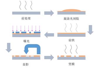
Figure 2
|
|
As shown in Fig. 3, the MA6 contact lithography machine produced by the Swiss company SUSS, and the MJB3 contact manual lithography machine produced by the company are shown in Fig. 4.
|
|
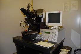 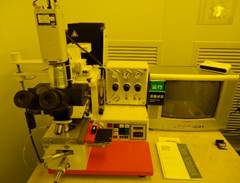
Figure3 Figure4
|
|
A typical contact lithography machine consists of a light source, a homogenizing optical path, an optical alignment system, a mask fixing, and a chip carrier. The light source usually uses a high-pressure mercury lamp or a high-power LED; the building block misplaced fly-eye lens and the homogenizing plate homogenize the light emitted by the light source; use the CCD or directly use the eyepiece to observe and adjust the alignment through the microscopic system; manual or automatic three-dimensional translation The table and the rotating table are used to fix and adjust the relative positions of the mask and the chip. The performance of the lithography machine is mainly reflected in three aspects: minimum resolution, engraving precision, and exposure uniformity.
At present, we are developing a small lithography machine suitable for laboratory use, and designing and fabricating its light source, uniform light path, alignment system, chip carrier, etc., which have begun to take shape.
|
|
Thickness controllable chip polishing machine
|
|
The basic method of mechanical polishing is to remove the material on the surface of the chip by mechanical grinding of abrasive grains in sandpaper or polishing liquid, and then obtain a smooth surface. This technology has a wide range of applications in large-scale integrated circuit manufacturing. At present, our research is mainly aimed at thinning, polishing, end face polishing and face polishing of small-sized chips.
The multilayer metal oxide technology of large-scale integrated circuits increases the unevenness of the surface of the chip, causing problems such as uneven thickness of the photoresist and reduced lithography precision. Mechanical polishing technology can improve the surface irregularities of the chip at a lower cost.
The basic principle of this technology is to remove the material on the surface of the sample by mechanically rubbing the surface of the sample with small, high-hardness particles (usually metal tungsten, metallic copper, diamond, etc.). A typical mechanical polishing apparatus consists of a polishing disk at the bottom, a polishing head that fixes the chip, and a channel that transports the slurry. The size of the polishing disk is larger than the size of the polishing head and the chip. During the polishing process, the rotation direction of the polishing disk is opposite to the rotation direction of the polishing head, but the rotation axes do not coincide, which are respectively referred to as the rotation and revolution of the polishing chip, as shown in FIG.
1.
At the same rotation speed, when the size of the abrasive particles is large, the material on the surface of the chip will be removed quickly, but the surface of the chip will be rough. Usually, the chip is thinned to a desired size with coarse abrasive grains. The thickness is then polished using fine abrasive particles to achieve the purpose of thinning the chip.
In the end face coupling of the chip, in order to improve the coupling efficiency, it is often necessary to polish the end face of the chip at a specific angle (typically 8°), which requires a special chip holder and a polishing head. Since the chip is mechanically rubbed close to the polishing plate in the process of polishing the end face, it is easy to cause cracking of the chip and damage of the surface device, so the jig and the polishing head of the chip need to have functions capable of protecting the chip and the surface device.
|
|
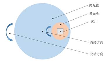
Figure 1. Schematic diagram of the working principle of the polishing machine图
|
|
In the 1980s, large international companies such as Motorola, Intel Pentium, and IBM invested heavily in research and commercial development. Today's major semiconductor and electronic equipment companies use this technology to process semiconductor components.
We have designed and manufactured a multi-function polishing head and polishing head spin mechanism. The multi-function polishing head can realize the thinning, polishing and end face polishing of wafers and chips below 2 inches, and the results can meet the needs of laboratory use.
|
|